Interface Science in Bimetallic Conductors
1. 引言
1.1 界面作为独立section
双金属导体中的界面不仅仅是两相之间的边界——它是一个具有独特性质的独立section:
创建界面section三维模型,可旋转查看原子结构
0:301.2 在双金属导体中的重要性
界面影响:
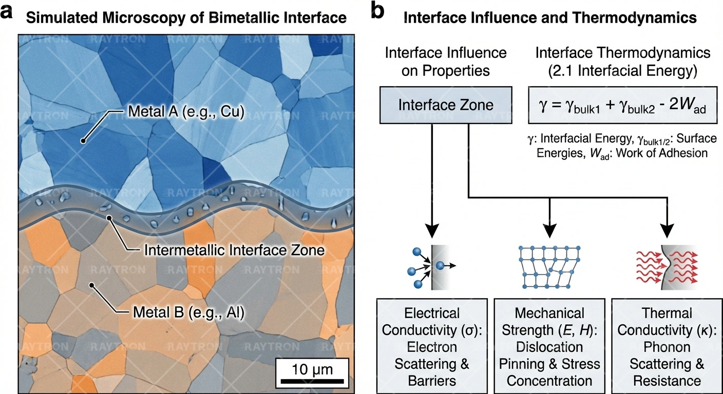
2. 界面热力学
2.1 界面能
金属-金属界面的能量可表示为:
其中:
- γA, γB = 金属A和B的Surface能
- Wad = 粘附功
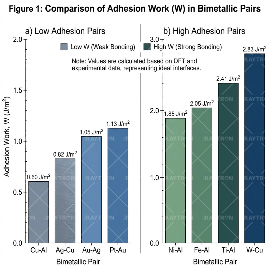
2.2 粘附功
粘附功代表分离界面所需的能量:
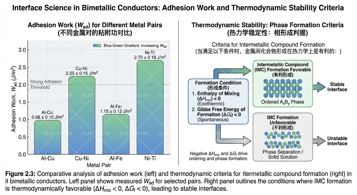
2.3 热力学稳定性
相形成判据:
当满足以下条件时,金属间化合物形成在热力学上是有利的:
3. 原子结构
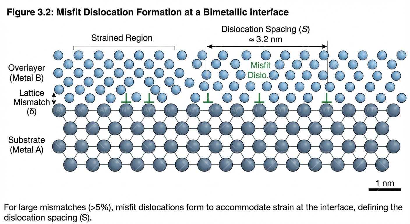
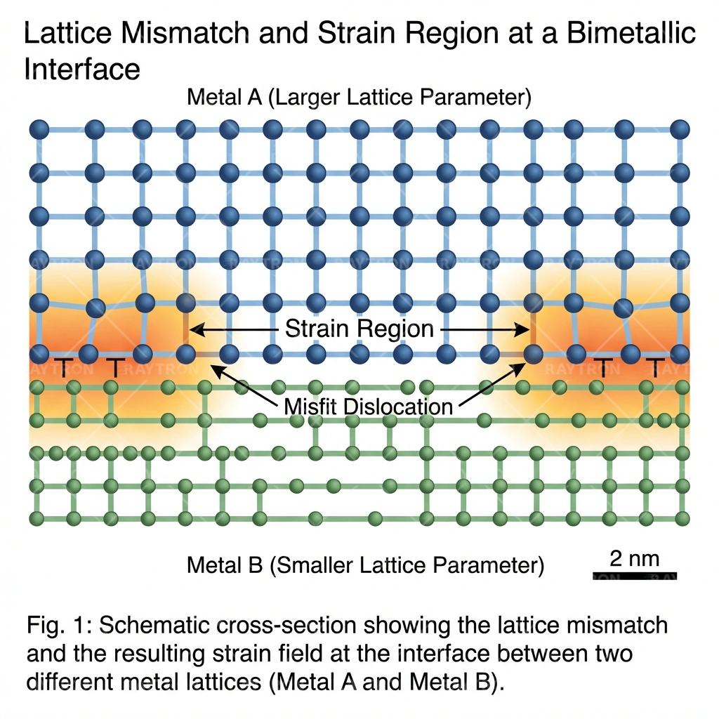
3.1 晶格失配
当两种不同晶格参数的金属相遇时,原子错配产生应变:
其中aA和aB是晶格参数。
3.2 失配位错
对于大失配(>5%),失配位错容纳应变:
创建失配位错形成动画
0:20位错间距:
其中b = 伯格斯矢量大小。
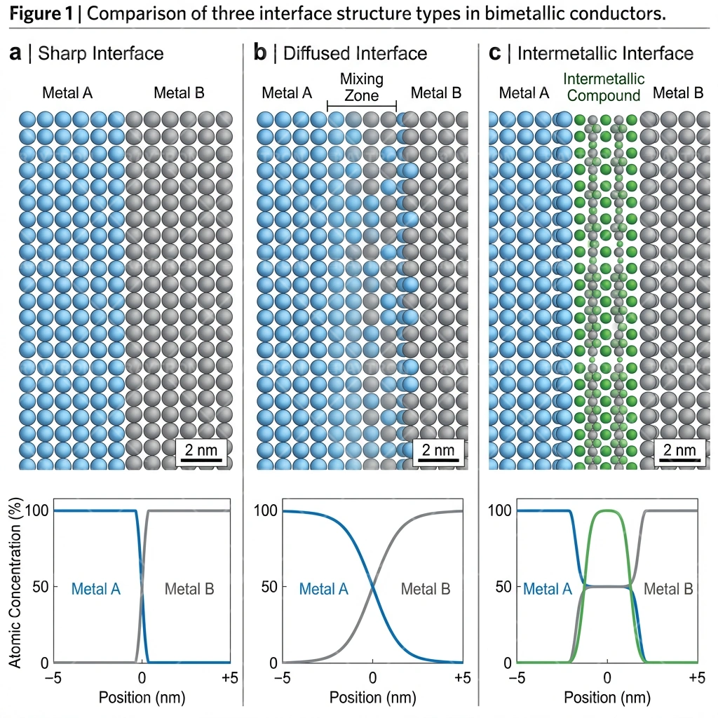
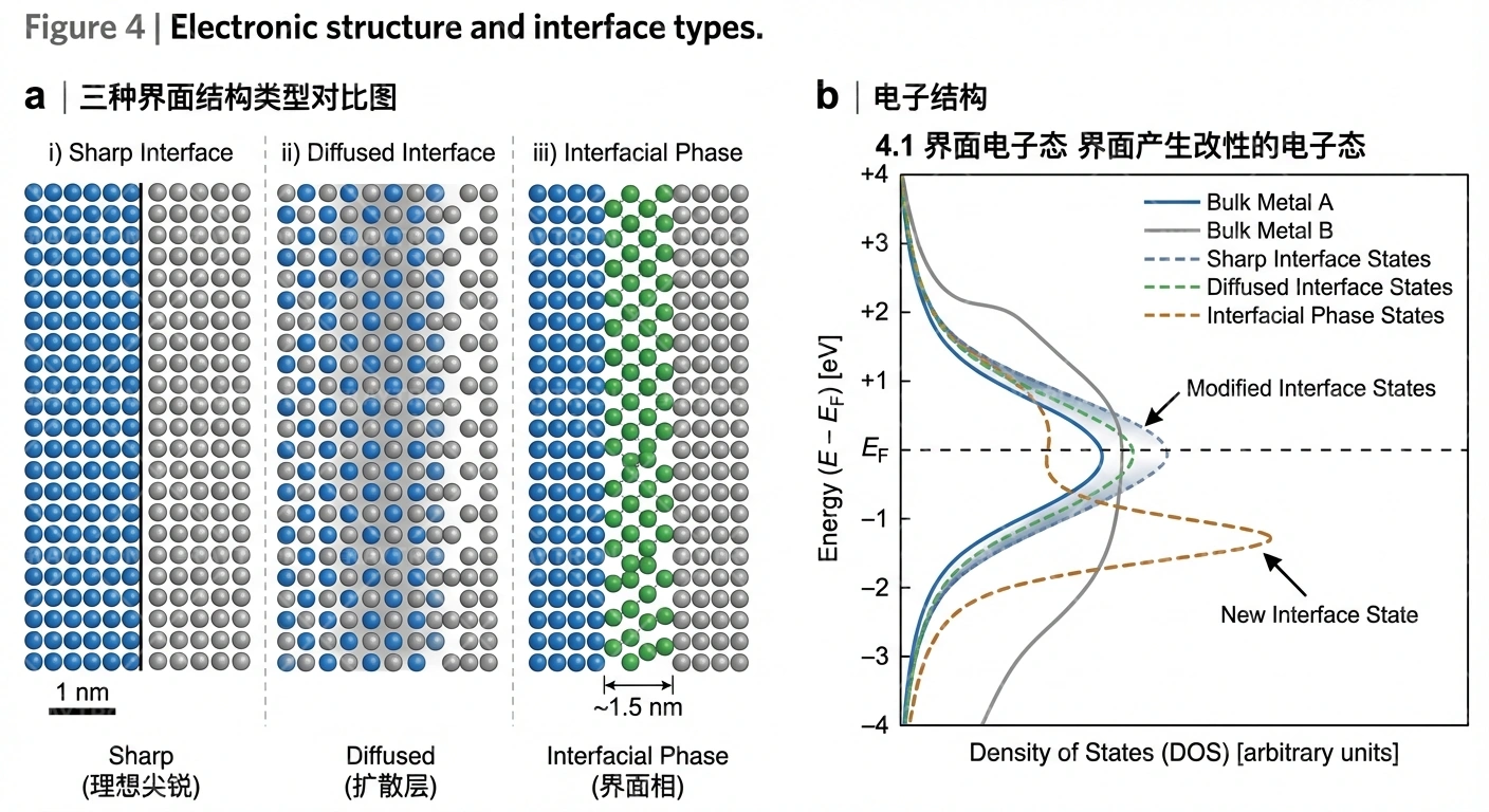
3.3 界面结构
三种界面结构类型:
4. 电子结构
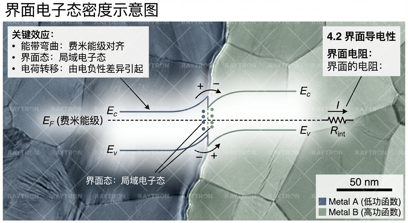
4.1 界面电子态
界面产生改性的电子态:
关键效应:
- 能带弯曲:费米能级对齐
- 界面态:局域电子态
- 电荷转移:由电负性差异引起
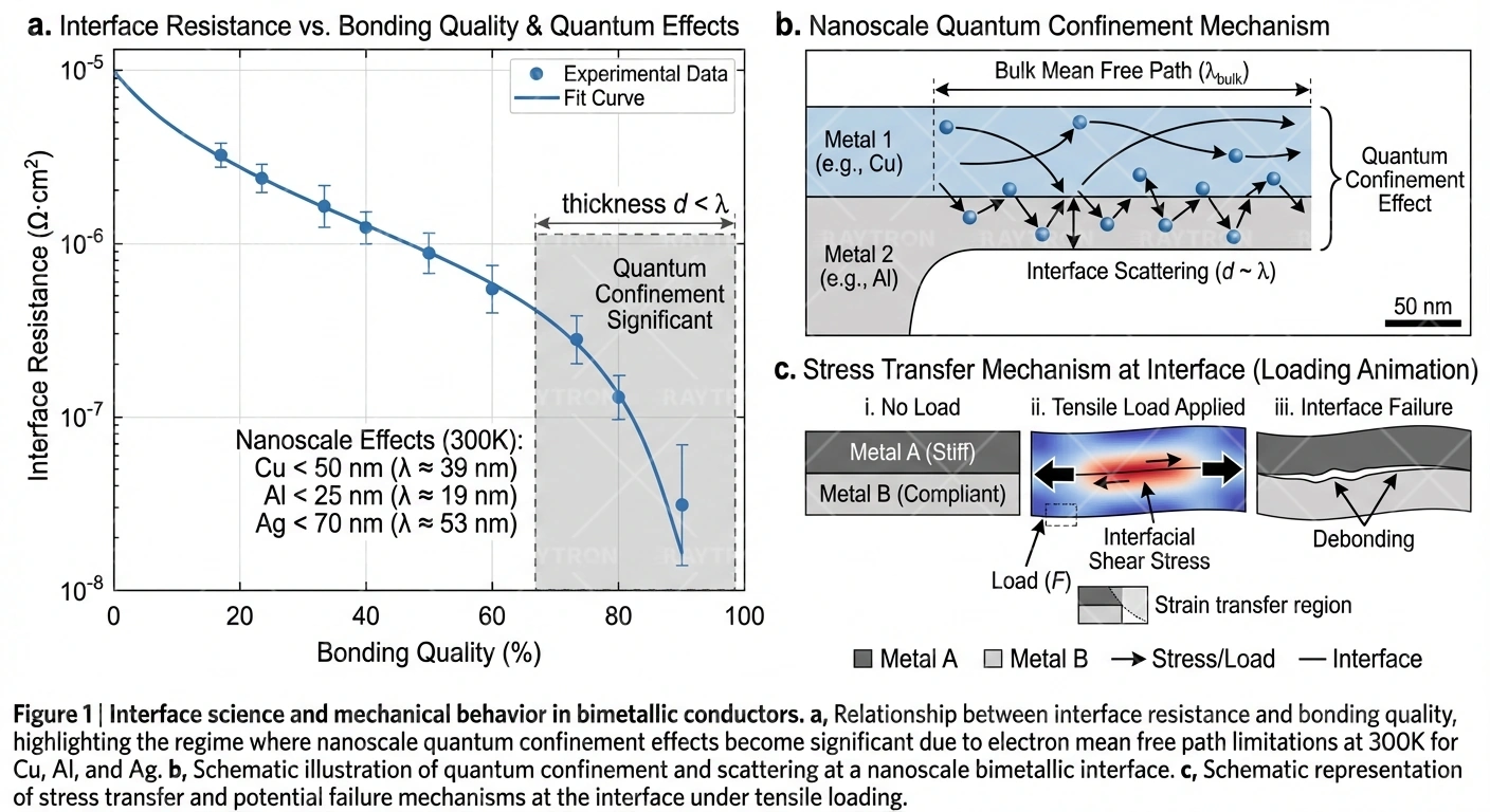
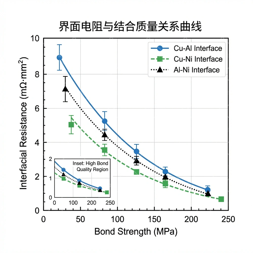
4.2 界面导电性
界面电阻:
界面的电阻:
4.3 纳米尺度量子效应
对于极薄层,量子限域效应变得显著:
平均自由程考虑:
- Cu: 39 nm (300K) - 对<50 nm层显著
- Al: 19 nm (300K) - 对<25 nm层显著
- Ag: 53 nm (300K) - 对<70 nm层显著
5. 力学行为
5.1 应力传递机制
界面实现层间载荷传递:
创建应力传递动画,展示加载时界面如何传递应力
0:30剪切滞后模型:
特征长度上的应力传递:
其中:
- τ = 界面剪应力
- P = 施加载荷
- d = 直径
- Lt = 传递长度
5.2 界面强度
理论强度:
其中Eeff是有效模量。
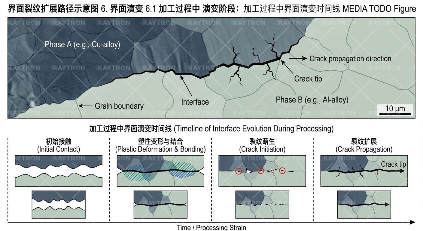
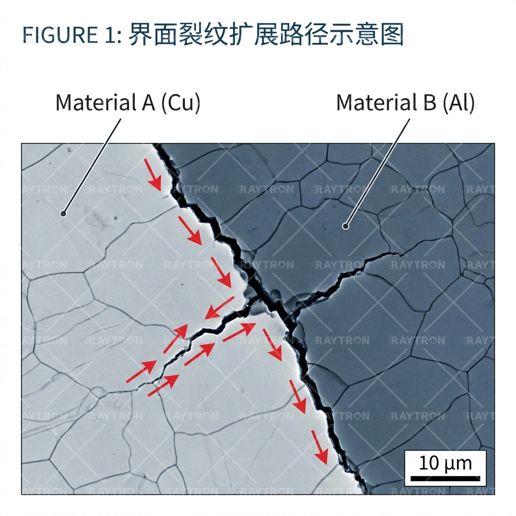
5.3 断裂行为
界面裂纹扩展:
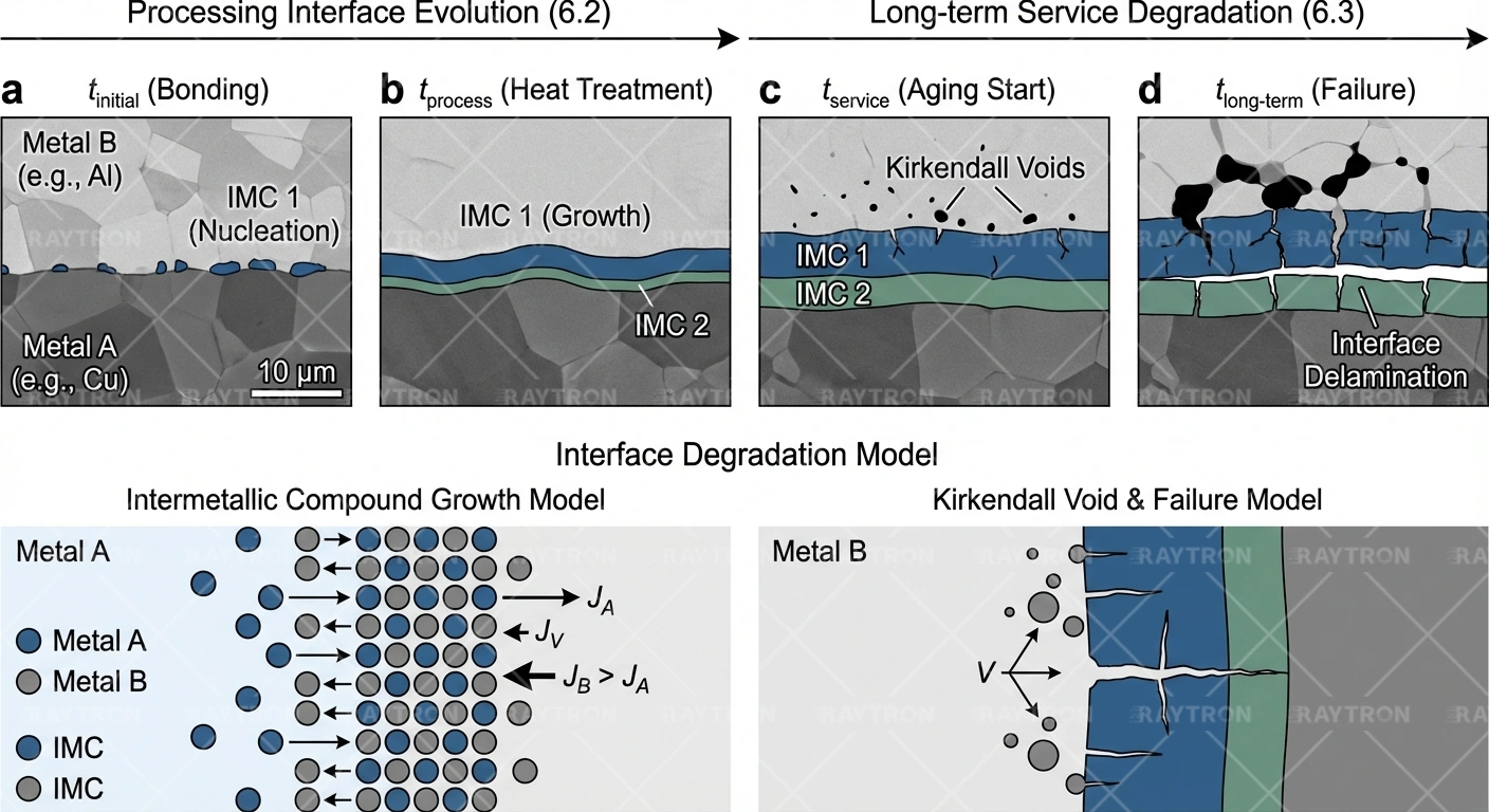
6. 界面演变
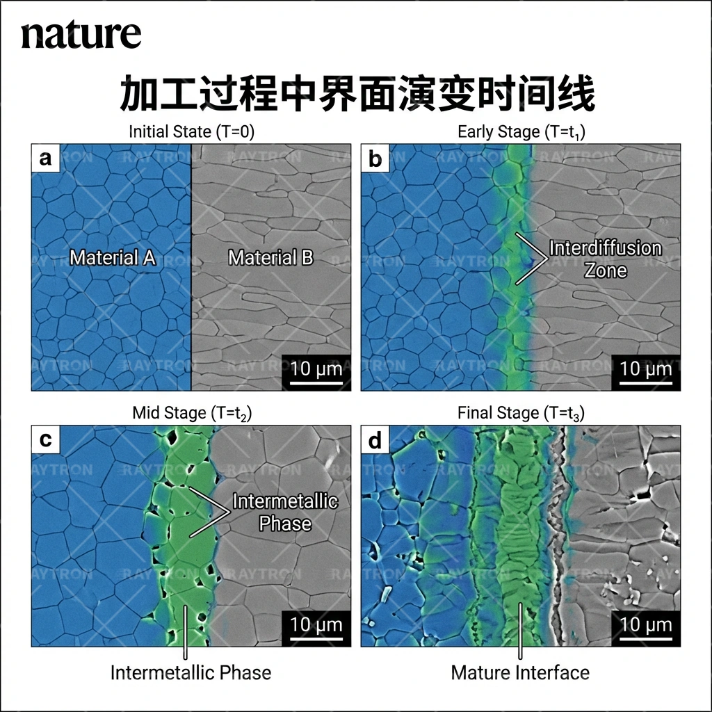
6.1 加工过程中
演变阶段:
6.2 服役过程中
长期演变:
6.3 界面退化模型
金属间化合物生长模型:
其中k通过阿伦尼乌斯关系取决于温度。
150°C服役温度下预测的IMC厚度:
- 1年: 0.3 μm
- 5年: 0.7 μm
- 10年: 1.0 μm
- 25年: 1.5 μm
7. 表征技术
7.1 显微方法
7.2 光谱方法
EDS线扫描分析:
7.3 力学测试
纳米压痕:
8. 建模方法
8.1 原子模拟
分子动力学:
Applications:
- 界面能计算
- 位错结构预测
- 变形机制研究
8.2 连续介质模型
有限元分析:
界面建模方法:
- 完美结合(共享节点)
- 内聚区模型
- 接触单元
8.3 多尺度方法
9. 工程意义
9.1 设计指南
9.2 质量控制指标
SPC参数:
- 界面电阻 (μΩ·cm²): USL 0.5, 目标 0.2
- 剥离强度 (MPa): USL 70, 目标 55, LSL 40
- IMC厚度 (μm): USL 3.0, 目标 2.0
- 结合覆盖率 (%): USL 100, 目标 98, LSL 95
9.3 未来方向
研究重点:
- 原位表征:实时观察界面演变
- 先进建模:机器学习加速性能预测
- 工程化界面:原子尺度设计
- 新材料组合:超越现有体系
Frequently Asked Questions
How does interface width affect bimetallic conductor performance?
Interface width affects electron scattering and stress transfer. Excessively wide interfaces (>100nm) increase resistance, while too narrow interfaces (<1nm) may result in insufficient bond strength. Optimal interface width of 1-10nm achieves balance between low resistance and high strength.
How to characterize bimetallic interface quality?
Main characterization methods include: SEM/TEM for interface morphology and atomic structure, EDS line scanning for composition distribution, peel testing for bond strength, and four-point probe for interface resistance. Combining these methods provides comprehensive interface quality assessment.
What changes occur at the interface during service?
At high temperatures, diffusion occurs at the interface leading to intermetallic compound growth; thermal cycling generates fatigue stress; current flow may cause electromigration. These changes are gradual, and high-quality interfaces can remain stable for over 25 years under normal operating conditions.
Why is Cu/Ni interface more stable than Cu/Al interface?
Cu and Ni form a continuous solid solution without brittle intermetallic compounds; small lattice mismatch (2.6%) results in low interface stress; high diffusion activation energy provides good high-temperature stability. In contrast, Cu/Al interface forms multiple brittle intermetallic compounds requiring strict temperature control during processing.
Figures
界面影响示意图,展示对导电、机械、热性能的影响
金属间化合物形成自由能图
晶格失配示意图,展示应变区
三种界面结构类型对比图
界面电子态Density示意图
界面电阻与结合质量关系曲线
界面裂纹扩展路径示意图
加工过程中界面演变时间线
IMC生长曲线,不同温度下
TEM界面图像,标注不同section
典型EDS线扫描结果
界面纳米压痕测试示意图
MD模拟界面结构截图
多尺度建模框架图
Tables
| 特征 | 体材料 | 界面section |
|---|---|---|
| 原子排列 | 规则晶体 | 无序/畸变 |
| 成分 | 均匀 | 梯度 |
| 电子结构 | 体能带 | 改性态 |
| 应力状态 | 近零 | 残余应力 |
| 宽度 | 不适用 | 1-100 nm |
| 金属 | Surface能 (mJ/m²) | 晶面 |
|---|---|---|
| Cu | 1.79 | (111) |
| Cu | 1.93 | (100) |
| Al | 1.14 | (111) |
| Al | 1.35 | (100) |
| Ni | 2.01 | (111) |
| Fe | 2.48 | (110) |
| 金属对 | W_ad (mJ/m²) | 键合特性 |
|---|---|---|
| Cu/Al | 520 | 金属键+some离子键 |
| Cu/Ni | 780 | 金属键(电负性相近) |
| Cu/Fe | 620 | 金属键 |
| Al/Fe | 480 | 金属键 |
| Ag/Cu | 680 | 金属键 |
| 化合物 | ΔG_formation | 热力学稳定? |
|---|---|---|
| CuAl₂ | -35 | 是 |
| Cu₉Al₄ | -28 | 是 |
| NiAl | -118 | 是 |
| FeAl | -52 | 是 |
| 金属对 | a_A (Å) | a_B (Å) | 失配 (%) |
|---|---|---|---|
| Cu/Al | 3.615 | 4.050 | -10.7% |
| Cu/Ni | 3.615 | 3.524 | +2.6% |
| Cu/Fe (fcc) | 3.615 | 3.591 | +0.7% |
| Al/Fe (bcc) | 4.050 | 2.866 | +41.2%* |
| 界面 | 失配 | 间距 (nm) |
|---|---|---|
| Cu/Al | 10.7% | 3.4 |
| Cu/Ni | 2.6% | 14.0 |
| Cu/Fe | 0.7% | 52.0 |
| 界面质量 | R_interface (μΩ·cm²) | 对总电阻影响 |
|---|---|---|
| 优秀 | <0.1 | <1% |
| 良好 | 0.1-0.5 | 1-3% |
| 一般 | 0.5-2.0 | 3-10% |
| 较差 | >2.0 | >10% |
| 材料 | σ_bulk (MPa) | σ_interface (MPa) | 比例 |
|---|---|---|---|
| CCA | 180 (Al芯) | 45-65 | 25-36% |
| CCS | 450 (钢) | 50-70 | 11-16% |
| NCC | 230 (Cu芯) | 55-75 | 24-33% |
| 环境 | 机制 | 效应 | 时间尺度 |
|---|---|---|---|
| 高温 | 扩散 | IMC生长 | 1000s-10000s h |
| 热循环 | CTE不匹配 | 疲劳 | 100s-1000s循环 |
| 电流 | 电迁移 | 成分变化 | 数年 |
| 腐蚀 | 电偶 | 界面侵蚀 | 数年 |
| 技术 | 尺度 | Info | 制备 |
|---|---|---|---|
| OM | >1 μm | 层结构、缺陷 | 抛光Cross-Section |
| SEM | 10 nm-1 μm | 界面形貌 | 抛光Cross-Section |
| TEM | 0.1-100 nm | 原子结构 | FIB减薄 |
| HRTEM | <1 nm | 原子柱 | FIB减薄 |
| STEM-EDS | 1-10 nm | 成分分布 | FIB减薄 |
| 方法 | 检测限 | 空间分辨率 | Info |
|---|---|---|---|
| EDS | 0.1 wt% | 1 μm | 主要元素 |
| WDS | 0.01 wt% | 1 μm | 微量元素 |
| 俄歇 | 0.1 at% | 50 nm | Surface成分 |
| XPS | 0.1 at% | 10 μm | 化学态 |
| 材料体系 | 势函数 | 系统尺寸 | 时间尺度 |
|---|---|---|---|
| Cu/Al | EAM | 10⁶原子 | 10 ns |
| Cu/Ni | EAM | 10⁵原子 | 1 ns |
| Cu/Fe | MEAM | 10⁵原子 | 1 ns |
| 要求 | 参数 | 目标 |
|---|---|---|
| 低电阻 | R_interface | <0.5 μΩ·cm² |
| High strength | 剥离强度 | >40 MPa |
| 稳定性 | IMC厚度 | <3 μm |
| 均匀性 | 结合覆盖率 | >95% |
References
- Surface free energies of solid metals Surface Science 62(1) , 267-276 (1977)
- Interfaces in Crystalline Materials Oxford University Press (1995)
- Interfaces in Materials Wiley (1997)
- Atomic structure of Cu/Al interfaces Physical Review B 64 , 045418 (2001)
- Grain boundary diffusion in metals Defect and Diffusion Forum 323 , 1-12 (2012)
- Theory of Dislocations (2nd ed.) Wiley (1982)
- Electronic Structure of Materials Oxford University Press (1996)
- Interface characterization in bimetallic wires Materials Characterization 152 , 148-158 (2019)
- In-situ TEM study of interface evolution Acta Materialia 185 , 175-185 (2020)
- Interface Analysis of High-Performance CCA Internal Report TR-2025-012 (2025)