Interface Science in Bimetallic Conductors
1. Introduction
1.1 Interfaceas section
Conductor Interfacenot only between ——has characteristics section:
section,
0:301.2 in Conductor important
InterfaceImpact:
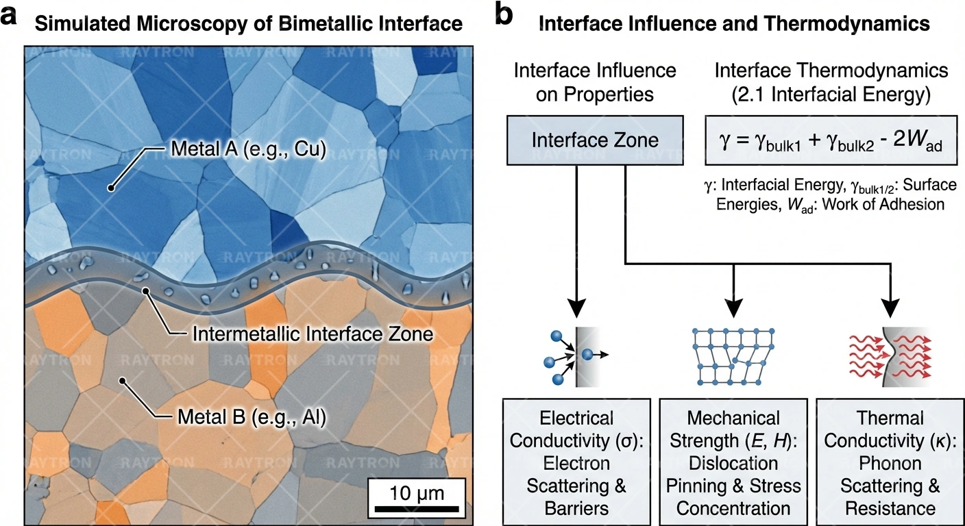
2. Interface Thermodynamics
2.1 Interface
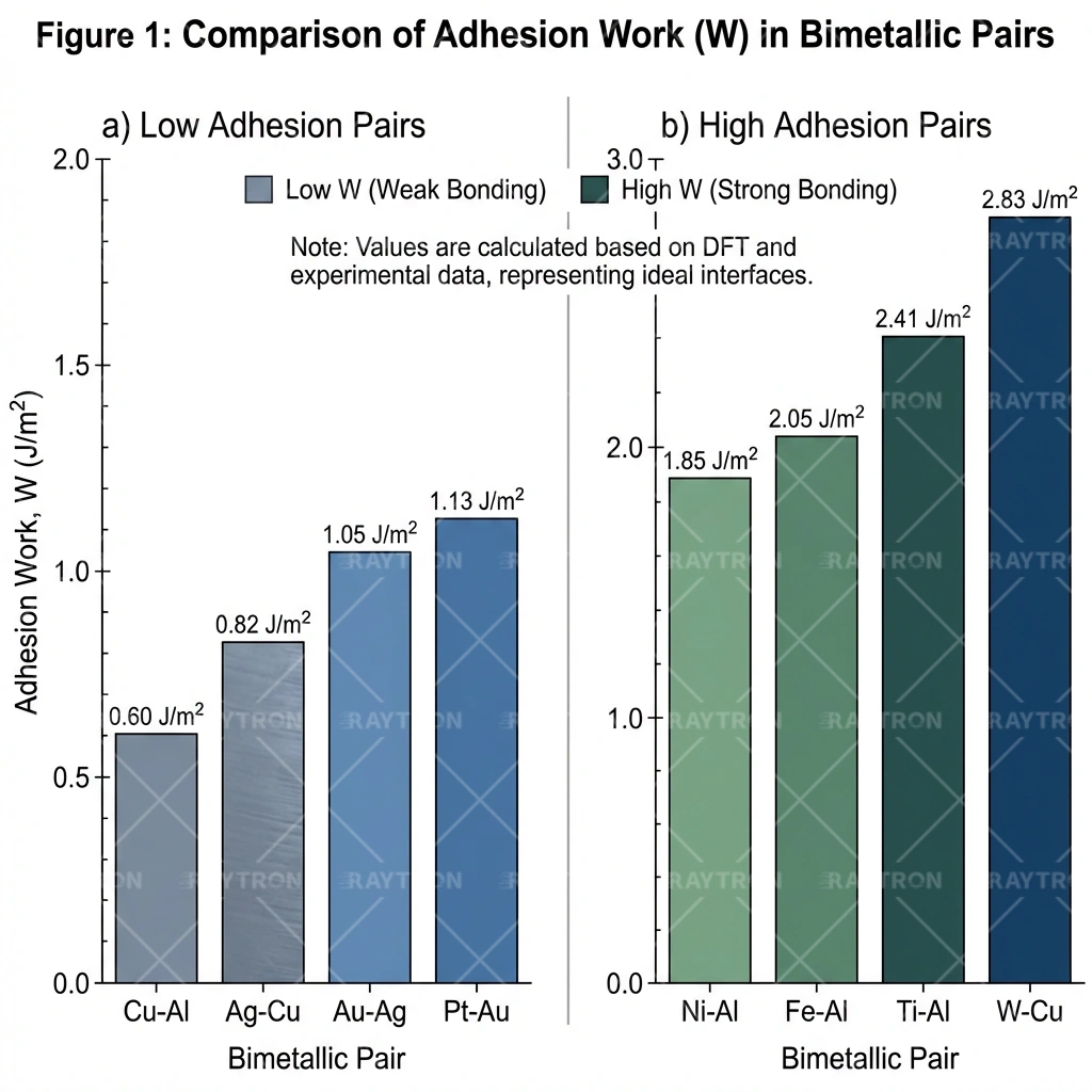
-Interface energy can as :
its :
- γA, γB = A and B Surface
- Wad =
2.2
Interfacerequires energy :
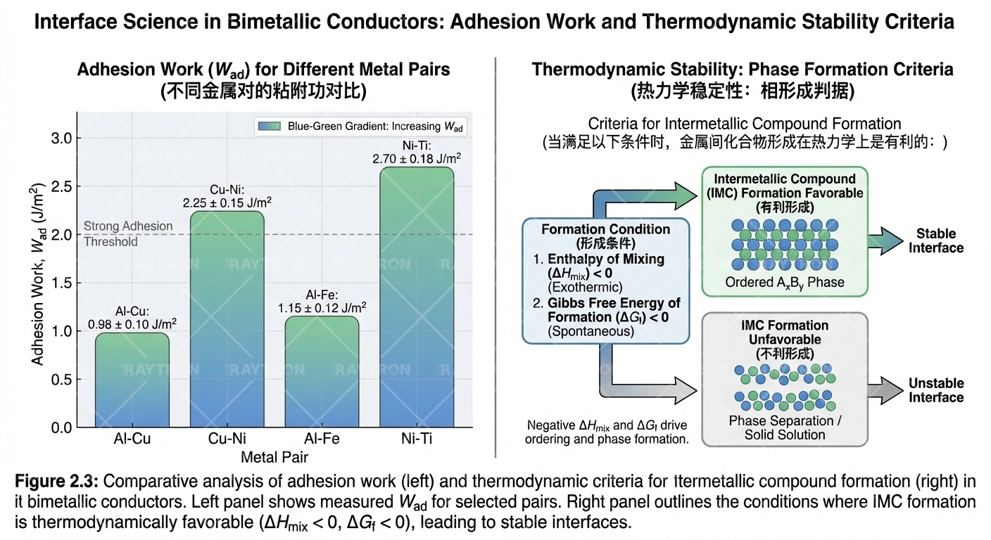
2.3 MechanicsStability
:
meets Conditions,in Mechanics :
3. Atomic Structure
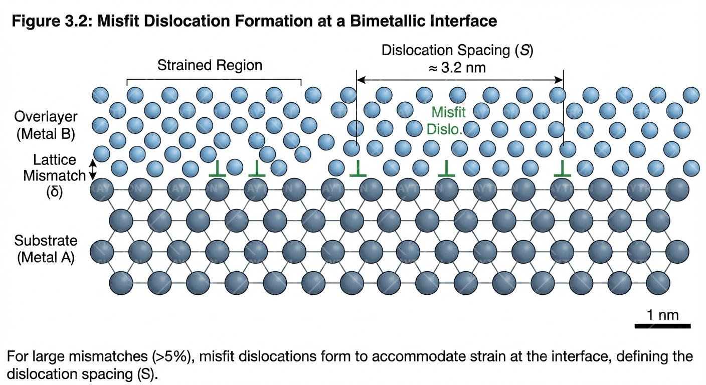
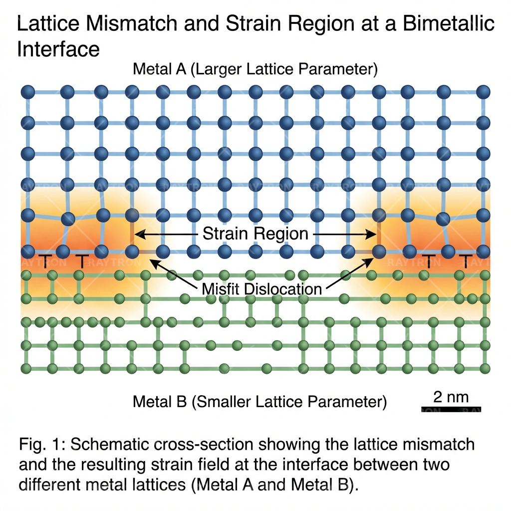
3.1
two different Parameter ,:
its aA and aBParameter。
3.2
for (>5%),:
animation
0:20:
its b = 。
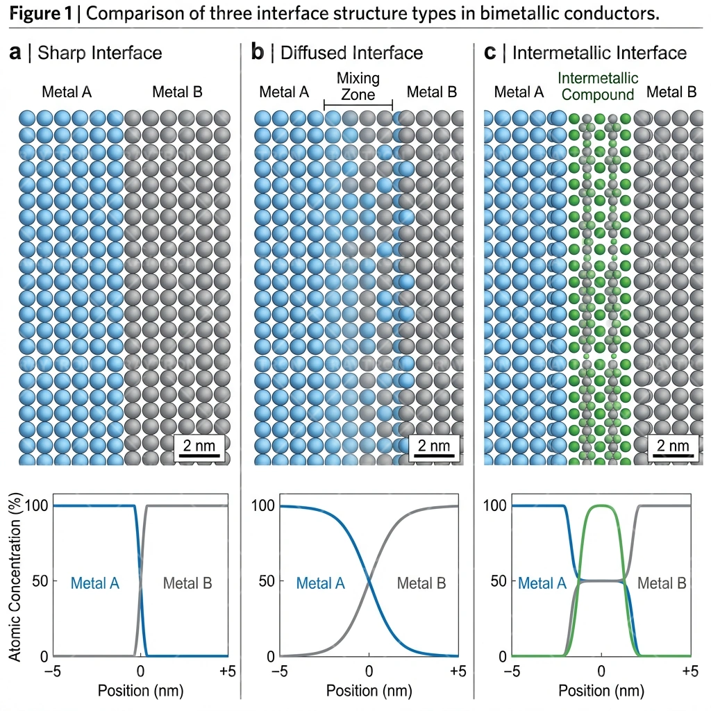
3.3 Interfacestructure
three Interfacestructure :
4.
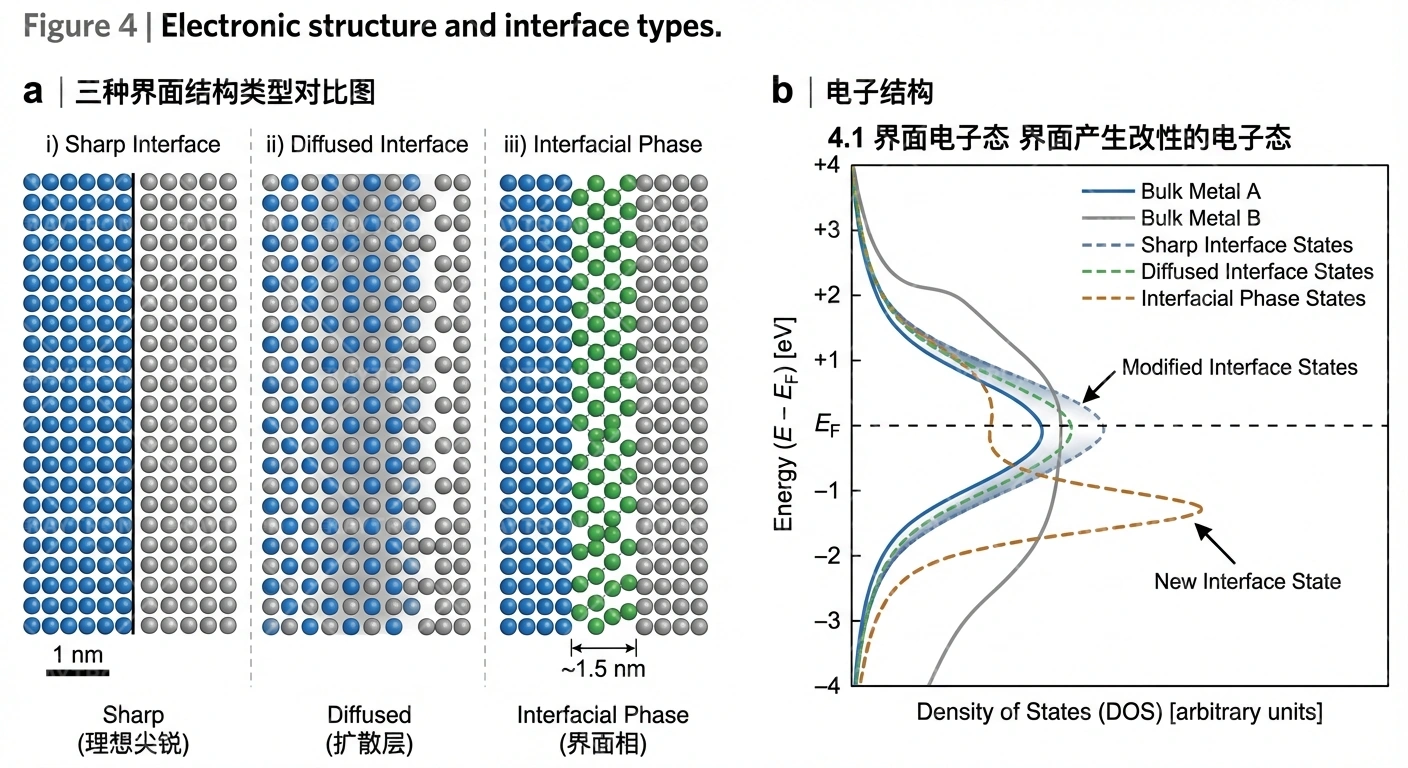
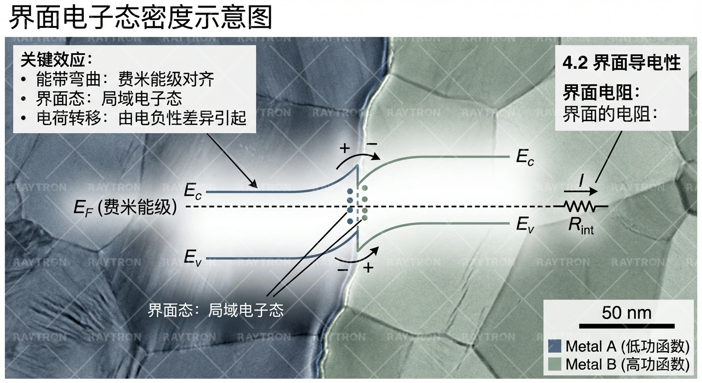
4.1 Interface
Interface :
Key:
- Bending:for
- Interface:
- :by
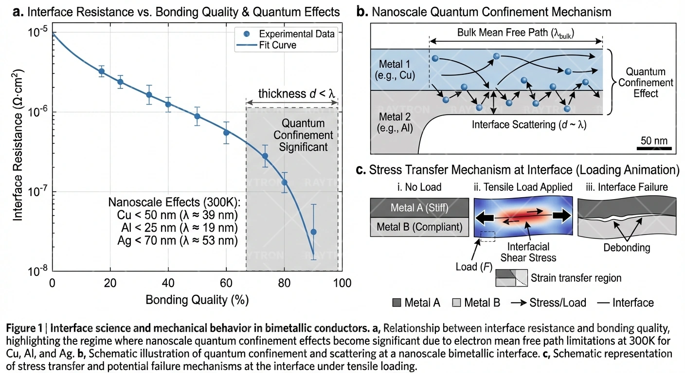
4.2 InterfaceConductivity
InterfaceResistance:
Interface Resistance:
4.3
for ,significant :
by :
- Cu: 39 nm (300K) - for <50 nmsignificant
- Al: 19 nm (300K) - for <25 nmsignificant
- Ag: 53 nm (300K) - for <70 nmsignificant
5.
5.1 Mechanism
Interfaceachieves :
animation,showing
0:30ShearModel:
Length :
its :
- τ = Interface
- P =
- d = Diameter
- Lt = Length
5.2 InterfaceStrength
TheoryStrength:
its EeffEffective。
5.3 Fractureas
InterfaceCrackExpansion:
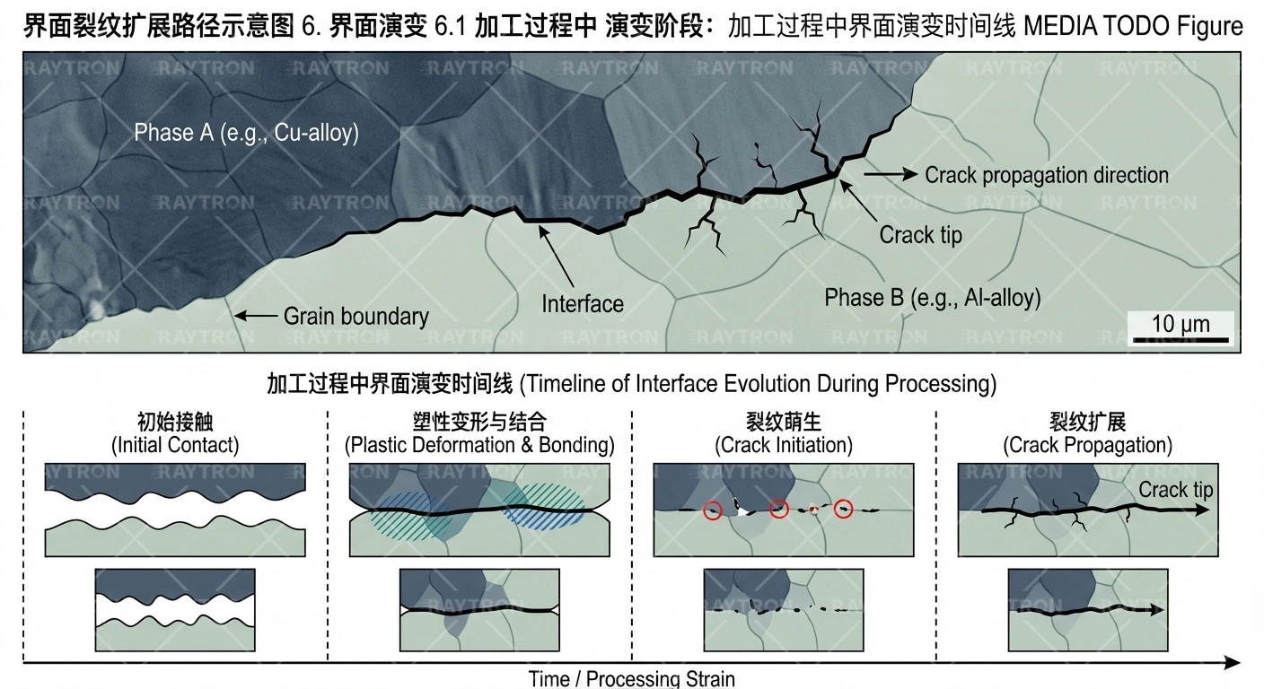
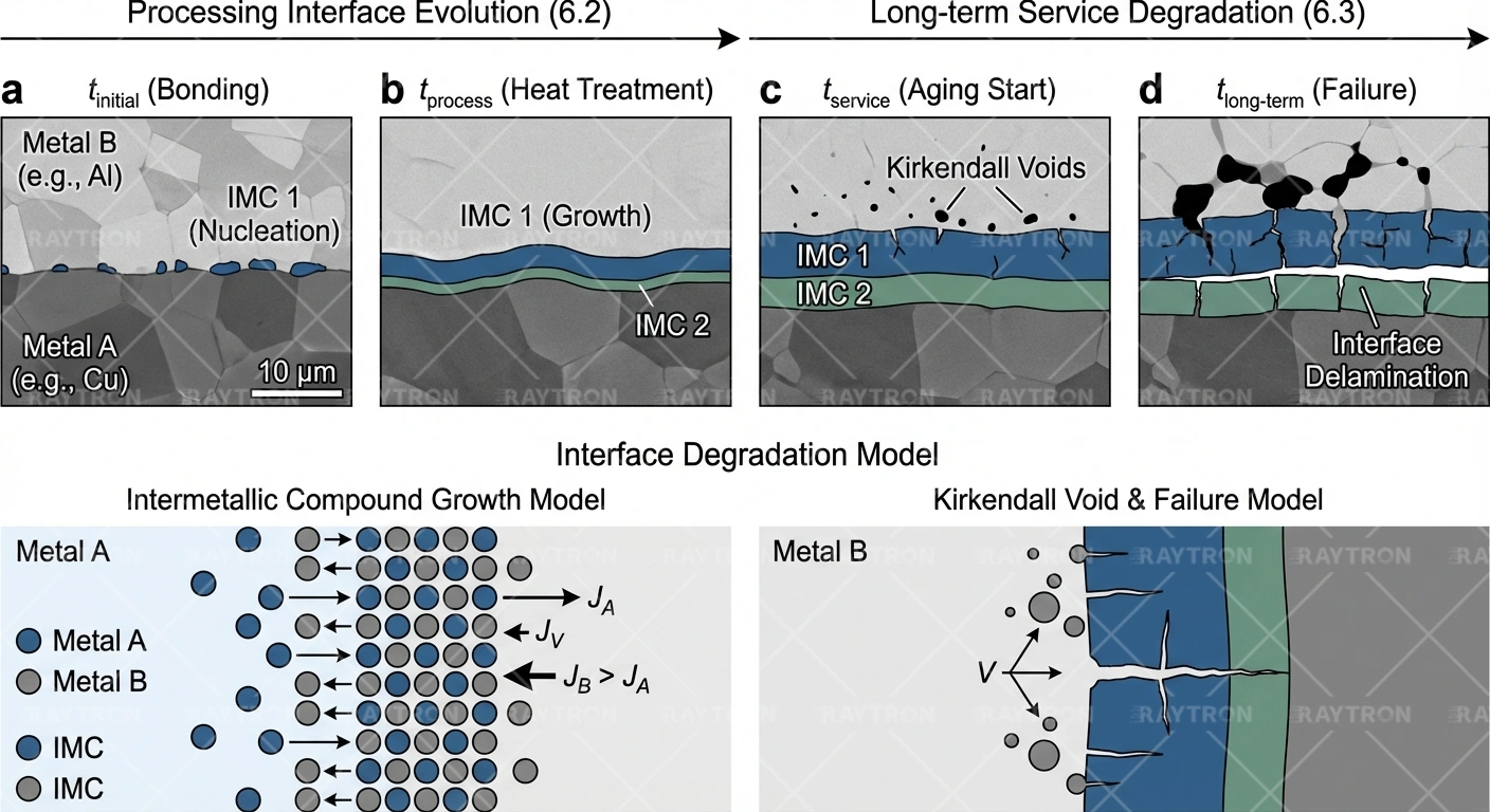
6. Interface Evolution
6.1 process
stage :
6.2 process
:
6.3 InterfaceDegradationModel
Model:
its kthrough temperature 。
150°Ctemperature Prediction IMCThickness:
- 1: 0.3 μm
- 5: 0.7 μm
- 10: 1.0 μm
- 25: 1.5 μm
7. Characterization
7.1 methods
7.2 methods
EDSanalysis:
7.3 MechanicsTesting
:
8. Modeling Methods
8.1 Simulation
Mechanics:
Applications:
- InterfaceCalculation
- structure Prediction
- DeformationMechanismresearch
8.2 Model
analysis:
InterfaceModelingMethods:
- ()
- Model
8.3 methods
9.
9.1 Design
9.2 Quality ControlIndicator
SPCParameter:
- InterfaceResistance (μΩ·cm²): USL 0.5, 0.2
- Strength (MPa): USL 70, 55, LSL 40
- IMCThickness (μm): USL 3.0, 2.0
- (%): USL 100, 98, LSL 95
9.3 future directions
research :
- :Interface
- Modeling:performancePrediction
- Interface:Design
- material:
Frequently Asked Questions
How does interface width affect bimetallic conductor performance?
Interface width affects electron scattering and stress transfer. Excessively wide interfaces (>100nm) increase resistance, while too narrow interfaces (<1nm) may result in insufficient bond strength. Optimal interface width of 1-10nm achieves balance between low resistance and high strength.
How to characterize bimetallic interface quality?
Main characterization methods include: SEM/TEM for interface morphology and atomic structure, EDS line scanning for composition distribution, peel testing for bond strength, and four-point probe for interface resistance. Combining these methods provides comprehensive interface quality assessment.
What changes occur at the interface during service?
At high temperatures, diffusion occurs at the interface leading to intermetallic compound growth; thermal cycling generates fatigue stress; current flow may cause electromigration. These changes are gradual, and high-quality interfaces can remain stable for over 25 years under normal operating conditions.
Why is Cu/Ni interface more stable than Cu/Al interface?
Cu and Ni form a continuous solid solution without brittle intermetallic compounds; small lattice mismatch (2.6%) results in low interface stress; high diffusion activation energy provides good high-temperature stability. In contrast, Cu/Al interface forms multiple brittle intermetallic compounds requiring strict temperature control during processing.
Figures
Interface Effect Diagram Showing Impact on Electrical, Mechanical, Thermal Properties
Intermetallic Compound Formation Free Energy Diagram
Lattice Mismatch Diagram, Showing Strain Zones
Three Interface Structure Types Comparison
Interface Electronic State Density Diagram
Interface Resistance vs Bond Quality Curve
Interface Crack Propagation Path Diagram
Interface Evolution Timeline During Processing
IMCGrowth Curves at Different Temperatures
TEM Interface Image with Zone Annotations
Typical EDS Line Scan Results
Interface Nanoindentation Test Diagram
MD Simulated Interface Structure Screenshot
Multi-Scale Modeling Framework Diagram
Tables
| Characteristic | Bulk Material | Interface Region |
|---|---|---|
| Atomic Arrangement | Regular Crystal | Disordered/Distorted |
| Composition | Uniform | Gradient |
| Electronic Structure | Bulk Band | Modified State |
| Stress State | Residual Stress | |
| Width | Non-Applicable | 1-100 nm |
| Metal | SurfaceCapacity (mJ/m²) | Crystal Plane |
|---|---|---|
| Cu | 1.79 | (111) |
| Cu | 1.93 | (100) |
| Al | 1.14 | (111) |
| Al | 1.35 | (100) |
| Ni | 2.01 | (111) |
| Fe | 2.48 | (110) |
| Metal on | W_ad (mJ/m²) | Key Special Properties |
|---|---|---|
| Cu/Al | 520 | Metallic + some Ionic Bonding |
| Cu/Ni | 780 | Metallic (Similar Electronic Properties) |
| Cu/Fe | 620 | Metallic Bonding |
| Al/Fe | 480 | Metallic Bonding |
| Ag/Cu | 680 | Metallic Bonding |
| Compound | ΔG_formation | ThermodynamicsStable? |
|---|---|---|
| CuAl₂ | -35 | is |
| Cu₉Al₄ | -28 | is |
| NiAl | -118 | is |
| FeAl | -52 | is |
| Metal on | a_A (Å) | a_B (Å) | Mismatch (%) |
|---|---|---|---|
| Cu/Al | 3.615 | 4.050 | -10.7% |
| Cu/Ni | 3.615 | 3.524 | +2.6% |
| Cu/Fe (fcc) | 3.615 | 3.591 | +0.7% |
| Al/Fe (bcc) | 4.050 | 2.866 | +41.2%* |
| Interface | Mismatch | Pitch (nm) |
|---|---|---|
| Cu/Al | 10.7% | 3.4 |
| Cu/Ni | 2.6% | 14.0 |
| Cu/Fe | 0.7% | 52.0 |
| Interface Quality | R_interface (μΩ·cm²) | on Total ResistanceImpact |
|---|---|---|
| Excellent | <0.1 | <1% |
| Good | 0.1-0.5 | 1-3% |
| General | 0.5-2.0 | 3-10% |
| ComparativelyPoor | >2.0 | >10% |
| Material | σ_bulk (MPa) | σ_interface (MPa) | RatioExample |
|---|---|---|---|
| CCA | 180 (AlCore) | 45-65 | 25-36% |
| CCS | 450 (Steel) | 50-70 | 11-16% |
| NCC | 230 (CuCore) | 55-75 | 24-33% |
| Environment | Mechanism | Effect | TimeScale |
|---|---|---|---|
| High Temperature | Diffusion | IMCGenerationLong | 1000s-10000s h |
| HotCycle | CTENon-Matching | Fatigue | 100s-1000sCycle |
| Current | Electric Migration | Composition Variation | CountYear |
| Corrosion | Galvanic | InterfaceErosion | CountYear |
| Technique | Scale | Info | Preparation |
|---|---|---|---|
| OM | >1 μm | Layer Structure & Defects | Polishing Cross-Section |
| SEM | 10 nm-1 μm | Interface Morphology | Polishing Cross-Section |
| TEM | 0.1-100 nm | Atomic Structure | FIB Reduced Thin |
| HRTEM | <1 nm | Atomic Column | FIB Reduced Thin |
| STEM-EDS | 1-10 nm | Composition Distribution | FIB Reduced Thin |
| Method | TestingLimit | Spatial Resolution Rate | Info |
|---|---|---|---|
| EDS | 0.1 wt% | 1 μm | Main Element |
| WDS | 0.01 wt% | 1 μm | Trace Element |
| AES | 0.1 at% | 50 nm | Surface Composition |
| XPS | 0.1 at% | 10 μm | Chemical State |
| MaterialSystem | PotentialCount | System Dimension | TimeScale |
|---|---|---|---|
| Cu/Al | EAM | 10⁶ Atomic | 10 ns |
| Cu/Ni | EAM | 10⁵ Atomic | 1 ns |
| Cu/Fe | MEAM | 10⁵ Atomic | 1 ns |
| Requirements | Parameter | Target |
|---|---|---|
| Low Resistance | R_interface | <0.5 μΩ·cm² |
| High strength | Peel Strength | >40 MPa |
| Stability | IMC Thicknessss | <3 μm |
| Uniform Properties | BondingCoverageRate | >95% |
References
- Surface free energies of solid metals Surface Science 62(1) , 267-276 (1977)
- Interfaces in Crystalline Materials Oxford University Press (1995)
- Interfaces in Materials Wiley (1997)
- Atomic structure of Cu/Al interfaces Physical Review B 64 , 045418 (2001)
- Grain boundary diffusion in metals Defect and Diffusion Forum 323 , 1-12 (2012)
- Theory of Dislocations (2nd ed.) Wiley (1982)
- Electronic Structure of Materials Oxford University Press (1996)
- Interface characterization in bimetallic wires Materials Characterization 152 , 148-158 (2019)
- In-situ TEM study of interface evolution Acta Materialia 185 , 175-185 (2020)
- Interface Analysis of High-Performance CCA Internal Report TR-2025-012 (2025)